

SEARCH WHAT YOU WANT
Ultrapure Water System for Semiconductor Manufacturing
Time:2026-08-15
Ultrapure water is essential for wafer rinsing, chip cleaning, etching, photolithography and other semiconductor manufacturing processes. Even trace levels of salts, particles, organic matter or microorganisms may contaminate wafer surfaces and reduce product yield.
A properly designed ultrapure water system for semiconductor manufacturing combines pretreatment, reverse osmosis, EDI and final polishing to provide stable high-purity water at the production point.
Why Semiconductor Manufacturing Requires Ultrapure Water
During semiconductor production, water comes into direct contact with wafers and electronic components. Untreated water may contain:
- Dissolved salts and silica
- Fine particles
- Organic contaminants
- Bacteria and endotoxins
- Dissolved gases
- Trace metals
These impurities can leave residues on wafer surfaces or interfere with sensitive manufacturing processes.
ASTM D5127 provides water-quality guidance for electronics and semiconductor manufacturing. The required purity must be selected according to the production process and measured at the point of distribution.
Typical Semiconductor Ultrapure Water Process
A typical process is:
Raw Water → Pretreatment → Double-Pass RO → EDI → UV Sterilization/TOC Reduction → Polishing Unit → Final Filter → Ultrapure Water Tank → Circulation Loop
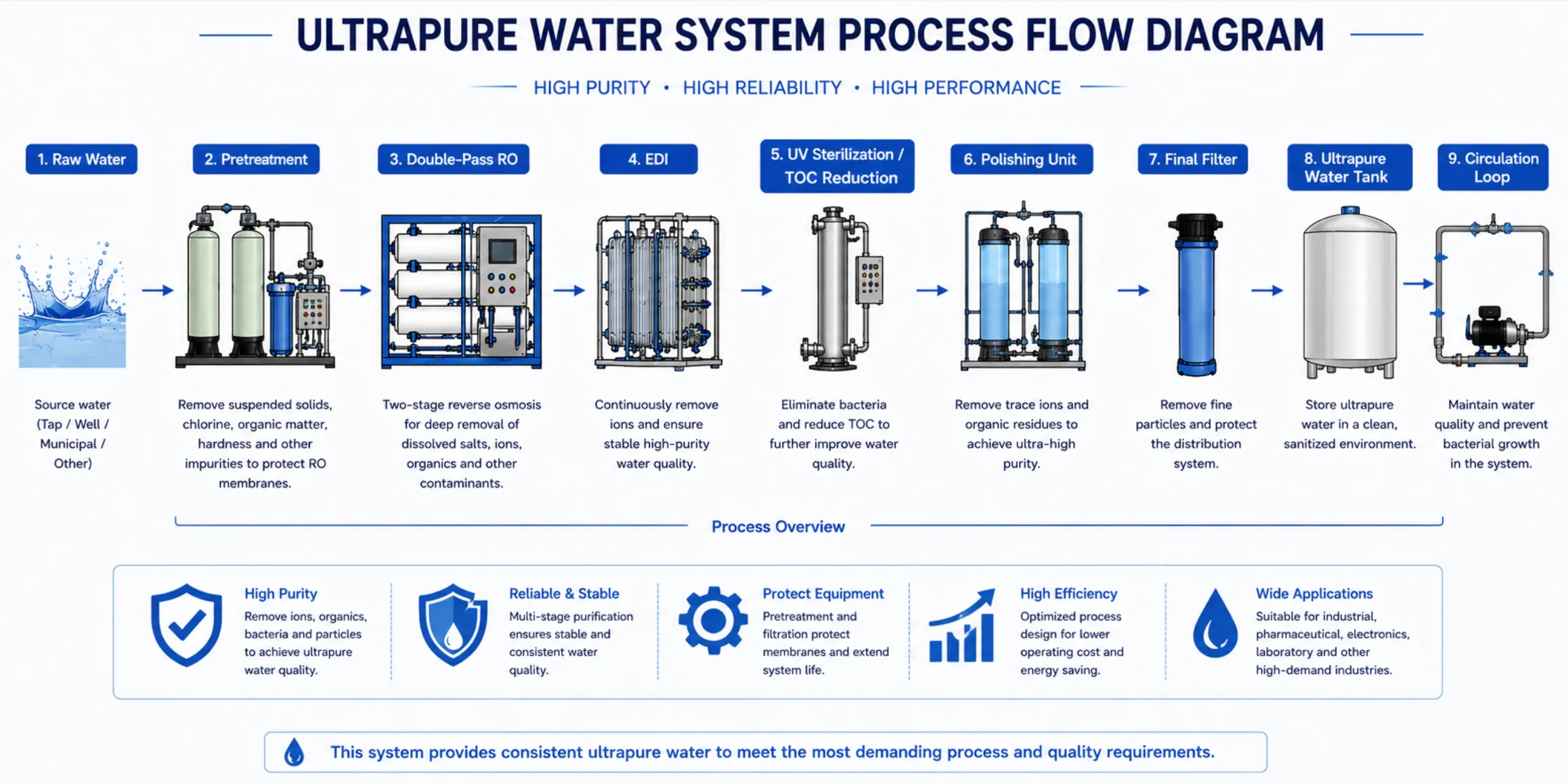
Pretreatment
Pretreatment removes suspended solids, chlorine, hardness and organic matter. Depending on the raw water quality, it may include:
- Multimedia or ultrafiltration system
- Activated carbon filtration
- Water softening or antiscalant dosing
- Cartridge filtration
Stable pretreatment protects the RO membranes and reduces system maintenance.
Double-Pass Reverse Osmosis
Double-pass RO removes most dissolved salts, silica, hardness and organic contaminants. It also provides suitable feedwater for the downstream EDI unit.
Compared with single-pass RO, double-pass RO normally provides lower conductivity and more stable water quality for semiconductor and electronics production.
EDI Polishing
An EDI ultrapure water system continuously removes residual ions from RO permeate.
EDI can produce high-purity water without frequent acid and alkali regeneration. Industrial EDI modules can achieve product-water resistivity up to approximately 18 MΩ·cm under suitable feedwater and operating conditions, according to the selected system design.
Final Polishing and Distribution
For higher-purity applications, additional treatment may include:
- UV oxidation for TOC reduction
- Mixed-bed polishing
- Membrane degassing
- Final ultrafiltration
- Sanitary storage tank
- Continuous circulation loop
The distribution system is as important as the purification equipment. Poor pipe design, stagnant sections or unsuitable materials may cause secondary contamination before the water reaches the production line.
Typical Water Quality Targets
| Parameter | Typical design target |
|---|---|
| Resistivity | Up to 18.2 MΩ·cm at 25°C |
| Conductivity | Down to approximately 0.055 μS/cm |
| TOC | Customized according to process |
| Silica | Very low or trace level |
| Particles | Controlled according to wafer process |
| Microorganisms | Strictly controlled |
These values are general references. The final standard should be based on the semiconductor process, wafer requirements and point-of-use specifications.
Key Design Considerations
A reliable RO EDI ultrapure water system for semiconductor plants should consider:
Raw Water Quality
The system must be designed according to TDS, hardness, silica, TOC, turbidity and microbial levels. A complete water analysis is required before equipment selection.
Required Capacity
Capacity should include production demand, peak consumption, circulation flow, cleaning water and future expansion. Selecting equipment only according to average daily demand may result in insufficient supply during peak production.
Stable Continuous Operation
Semiconductor factories normally require continuous and stable water supply. Recommended options include:
- Automatic PLC control
- Online resistivity monitoring
- TOC and flow monitoring
- Duty and standby pumps
- Automatic alarm system
- Remote monitoring
- Backup treatment units
Distribution Loop
Ultrapure water should circulate continuously through a properly designed pipeline. Stainless steel or high-purity polymer piping may be selected according to the required water standard and project budget.
Applications
Semiconductor and electronics ultrapure water systems are commonly used for:
- Semiconductor wafer rinsing
- Integrated circuit manufacturing
- PCB production
- Microelectronics cleaning
- LED manufacturing
- Photovoltaic cell production
- Precision electronic components
- Laboratory process water
View our semiconductor water treatment solutions and electronics factory water treatment applications for related system configurations.
Optional Configurations
Zhongnuo can customize semiconductor ultrapure water systems with:
- Single-pass or double-pass RO
- EDI polishing
- UV sterilization and TOC reduction
- Mixed-bed ion exchange
- Membrane degassing
- Final ultrafiltration
- Automatic CIP cleaning
- Online conductivity and resistivity monitoring
- Constant-pressure circulation
- Fully automatic PLC control
Information Required for a Quotation
To prepare an accurate solution, please provide:
- Raw water analysis report
- Required ultrapure water capacity
- Required resistivity or conductivity
- TOC, silica and particle requirements
- Daily operating hours
- Final water application
- Local voltage and frequency
- Available installation space
- Distribution-loop requirements
Frequently Asked Questions
Is RO water sufficient for semiconductor manufacturing?
RO water may be suitable for general electronics cleaning, but advanced semiconductor processes usually require EDI and additional polishing to achieve lower ionic, organic and particle levels.
Why is double-pass RO used before EDI?
Double-pass RO reduces salts, silica and carbon dioxide entering the EDI unit, helping improve product-water stability and EDI operating life.
Can an EDI system produce 18.2 MΩ·cm water?
EDI can produce water approaching 18 MΩ·cm under suitable feedwater conditions. Achieving stable 18.2 MΩ·cm water at the point of use may require additional polishing and a properly designed circulation loop.
How is system capacity calculated?
Capacity should be based on peak hourly demand, production shifts, cleaning consumption, circulation requirements and future factory expansion.
Conclusion
An effective ultrapure water system for semiconductor manufacturing requires more than RO and EDI equipment. Pretreatment, final polishing, online monitoring and the distribution loop must work together to maintain stable water quality.
Contact Zhongnuo Water Treatment for a customized semiconductor ultrapure water system design and quotation.
Ultrapure water is essential for wafer rinsing, chip cleaning, etching, photolithography and other semiconductor manufacturing processes. Even trace levels of salts, particles, organic matter or microorganisms may contaminate wafer surfaces and reduce product yield.
A properly designed ultrapure water system for semiconductor manufacturing combines pretreatment, reverse osmosis, EDI and final polishing to provide stable high-purity water at the production point.
Why Semiconductor Manufacturing Requires Ultrapure Water
During semiconductor production, water comes into direct contact with wafers and electronic components. Untreated water may contain:
- Dissolved salts and silica
- Fine particles
- Organic contaminants
- Bacteria and endotoxins
- Dissolved gases
- Trace metals
These impurities can leave residues on wafer surfaces or interfere with sensitive manufacturing processes.
ASTM D5127 provides water-quality guidance for electronics and semiconductor manufacturing. The required purity must be selected according to the production process and measured at the point of distribution.
Typical Semiconductor Ultrapure Water Process
A typical process is:
Raw Water → Pretreatment → Double-Pass RO → EDI → UV Sterilization/TOC Reduction → Polishing Unit → Final Filter → Ultrapure Water Tank → Circulation Loop
Pretreatment
Pretreatment removes suspended solids, chlorine, hardness and organic matter. Depending on the raw water quality, it may include:
- Multimedia or ultrafiltration system
- Activated carbon filtration
- Water softening or antiscalant dosing
- Cartridge filtration
Stable pretreatment protects the RO membranes and reduces system maintenance.
Double-Pass Reverse Osmosis
Double-pass RO removes most dissolved salts, silica, hardness and organic contaminants. It also provides suitable feedwater for the downstream EDI unit.
Compared with single-pass RO, double-pass RO normally provides lower conductivity and more stable water quality for semiconductor and electronics production.
EDI Polishing
An EDI ultrapure water system continuously removes residual ions from RO permeate.
EDI can produce high-purity water without frequent acid and alkali regeneration. Industrial EDI modules can achieve product-water resistivity up to approximately 18 MΩ·cm under suitable feedwater and operating conditions, according to the selected system design.
Final Polishing and Distribution
For higher-purity applications, additional treatment may include:
- UV oxidation for TOC reduction
- Mixed-bed polishing
- Membrane degassing
- Final ultrafiltration
- Sanitary storage tank
- Continuous circulation loop
The distribution system is as important as the purification equipment. Poor pipe design, stagnant sections or unsuitable materials may cause secondary contamination before the water reaches the production line.
Typical Water Quality Targets
| Parameter | Typical design target |
|---|---|
| Resistivity | Up to 18.2 MΩ·cm at 25°C |
| Conductivity | Down to approximately 0.055 μS/cm |
| TOC | Customized according to process |
| Silica | Very low or trace level |
| Particles | Controlled according to wafer process |
| Microorganisms | Strictly controlled |
These values are general references. The final standard should be based on the semiconductor process, wafer requirements and point-of-use specifications.
Key Design Considerations
A reliable RO EDI ultrapure water system for semiconductor plants should consider:
Raw Water Quality
The system must be designed according to TDS, hardness, silica, TOC, turbidity and microbial levels. A complete water analysis is required before equipment selection.
Required Capacity
Capacity should include production demand, peak consumption, circulation flow, cleaning water and future expansion. Selecting equipment only according to average daily demand may result in insufficient supply during peak production.
Stable Continuous Operation
Semiconductor factories normally require continuous and stable water supply. Recommended options include:
- Automatic PLC control
- Online resistivity monitoring
- TOC and flow monitoring
- Duty and standby pumps
- Automatic alarm system
- Remote monitoring
- Backup treatment units
Distribution Loop
Ultrapure water should circulate continuously through a properly designed pipeline. Stainless steel or high-purity polymer piping may be selected according to the required water standard and project budget.
Applications
Semiconductor and electronics ultrapure water systems are commonly used for:
- Semiconductor wafer rinsing
- Integrated circuit manufacturing
- PCB production
- Microelectronics cleaning
- LED manufacturing
- Photovoltaic cell production
- Precision electronic components
- Laboratory process water
View our semiconductor water treatment solutions and electronics factory water treatment applications for related system configurations.
Optional Configurations
Zhongnuo can customize semiconductor ultrapure water systems with:
- Single-pass or double-pass RO
- EDI polishing
- UV sterilization and TOC reduction
- Mixed-bed ion exchange
- Membrane degassing
- Final ultrafiltration
- Automatic CIP cleaning
- Online conductivity and resistivity monitoring
- Constant-pressure circulation
- Fully automatic PLC control
Information Required for a Quotation
To prepare an accurate solution, please provide:
- Raw water analysis report
- Required ultrapure water capacity
- Required resistivity or conductivity
- TOC, silica and particle requirements
- Daily operating hours
- Final water application
- Local voltage and frequency
- Available installation space
- Distribution-loop requirements
Frequently Asked Questions
Is RO water sufficient for semiconductor manufacturing?
RO water may be suitable for general electronics cleaning, but advanced semiconductor processes usually require EDI and additional polishing to achieve lower ionic, organic and particle levels.
Why is double-pass RO used before EDI?
Double-pass RO reduces salts, silica and carbon dioxide entering the EDI unit, helping improve product-water stability and EDI operating life.
Can an EDI system produce 18.2 MΩ·cm water?
EDI can produce water approaching 18 MΩ·cm under suitable feedwater conditions. Achieving stable 18.2 MΩ·cm water at the point of use may require additional polishing and a properly designed circulation loop.
How is system capacity calculated?
Capacity should be based on peak hourly demand, production shifts, cleaning consumption, circulation requirements and future factory expansion.
Conclusion
An effective ultrapure water system for semiconductor manufacturing requires more than RO and EDI equipment. Pretreatment, final polishing, online monitoring and the distribution loop must work together to maintain stable water quality.
Contact Zhongnuo Water Treatment for a customized semiconductor ultrapure water system design and quotation.
Get a Quote for Free
Submit this form and our sales representative will contact you soon.


ONLINE MESSAGE
Copyright © 2026 Zhongnuo Water Treatment Co., Ltd.